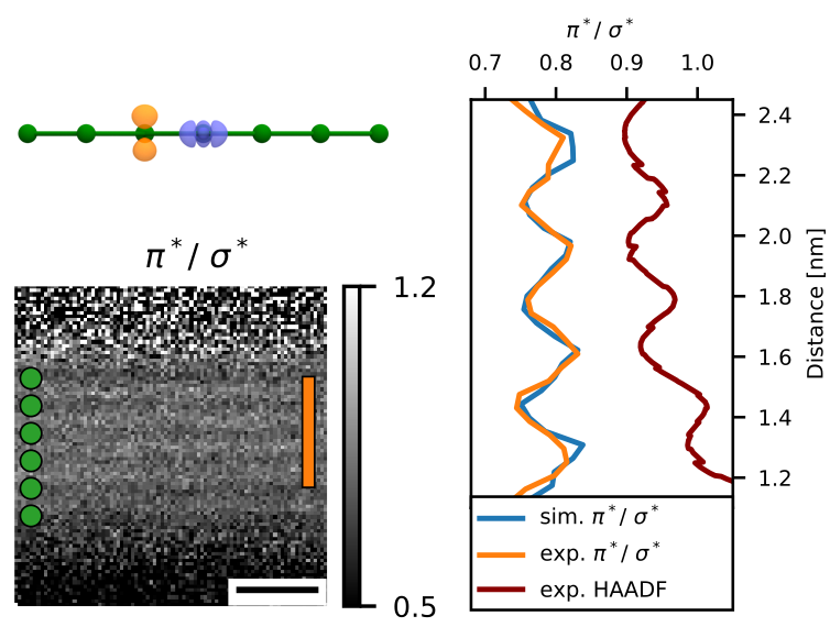
On the left, a mapping of electronic states at the nanometer scale. The green circles correspond to the position of the atomic planes with respect to the signal (General terms A signal is a simplified and generally coded message. There is…) transmission electron microscope (HAADF).
On the right, the profile of the electronic states and of the HAADF signal.
© Bugnet et al.
Crystalline materials exhibit a regular structure held together by chemical bonds. These bonds can be found in different electronic states which govern most of the physical and chemical properties of crystalline materials. The electronic states at the level of defects, interfaces and surfaces influence the macroscopic properties of the crystal (Crystal is a common term for a regular-shaped solid, though…)making it essential to know these electronic states.
Researchers from the Materials, Engineering and Science laboratory (MATEIS, CNRS/INSA Lyon/Université Claude Bernard (Claude Bernard, born July 12, 1813 in Saint-Julien (Rhône) and died on…) Lyon 1), the SuperSTEM laboratory (United Kingdom), the universities of Leeds and York (United Kingdom), theuniversity (A university is an institution of higher education whose objective is the…) of technology (The word technology has two de facto meanings:) of Vienna (Austria) and the University of West Virginia (USA) succeeded in mapping the electronic states of graphene layers by loss spectroscopy.energy (In common sense, energy designates everything that allows you to do work, make energy, etc.) electrons, a technique that works in a transmission electron microscope. So far these data (In information technology (IT), data is an elementary description, often…) were drowned in noise (In its ordinary meaning, the word noise comes close to the main meaning of the word sound….) and artifacts related to the measurement technique.
Graphene was chosen as a model because its properties and spectral characteristics are well known. The scientists here focused on a sample (Generally speaking, a sample is a small amount of material, information, or…) consisting of several stacked and loosely bonded graphene sheets. They developed an approach that relies on numerical calculations and experimental data, taken in a transmission electron microscope, from which maps of electronic states can be interpreted in terms of atomic orbitals.
The team was thus able to distinguish and remove the beam propagation contributions fromelectron (The electron is an elementary particle of the lepton family, and has a charge…), due among other things to the thickness of the sample, harmful to the interpretation of the contrast. She thus obtained a precise mapping of the electronic states of graphene. This work is of significant methodological interest for understanding the role of chemical bonds at interfaces and defects in solids, and thus promoting the creation of new materials intended for example for the microelectronics of the future, which relies heavily on the properties of graphene.
References:
Imaging the spatial distribution of electronic states in graphene using electron energy-loss spectroscopy: prospect of orbital mapping.
M. Bugnet, M. Ederer, VK Lazarov, L. Li, QM Ramasse, S. Löffler, and DM Kepaptsoglou.
Physical Review Letters128, 116401 (2022).
doi.org/10.1103/PhysRevLett.128.116401
Article available on the HAL open archive database
Did you like this article? Do you wish to support us ? Share it on social networks with your friends and/or comment on it, this will encourage us to publish more similar topics!
#cartography #electronic #states #graphene


